Home/Service/PCB Assembly

PCB Assembly

Our advanced PCB assembly equipment and mature manufacturing processes deliver outstanding technical capability, stable quality and high efficiency within the EMS industry.
We have certified IPC-A-610 trainers working alongside production operators to guarantee all assembled PCBs meet premium international quality standards.

SMT Basic Process:

  • Solder Paste Printing
  • Component Placement
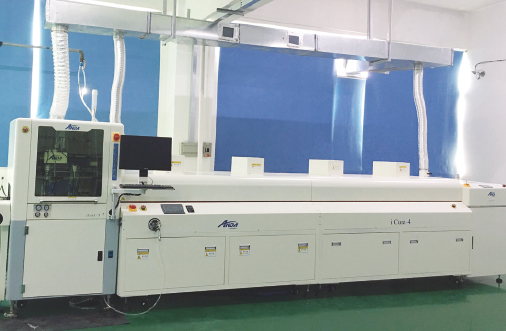
  • Reflow Soldering
  • Board Rework & Repair

Our PCBA Advantages:

Strong engineering support: Front-end engineering & dedicated test engineering teams
Premium imported raw materials: We adopt Japanese KOKI solder paste and high-grade solder wire; refurbished/secondary raw materials are strictly prohibited
Rigorous quality control: Pre-reflow QC inspection, defect screening, and 100% post-reflow PCBA inspection
Comprehensive service system: Responsive customer support, on-time delivery with guaranteed quality to continuously fulfil customer requirements
Professional quality team: Experienced and well-trained quality control personnel
Raw material management: Complete incoming material verification before production launch
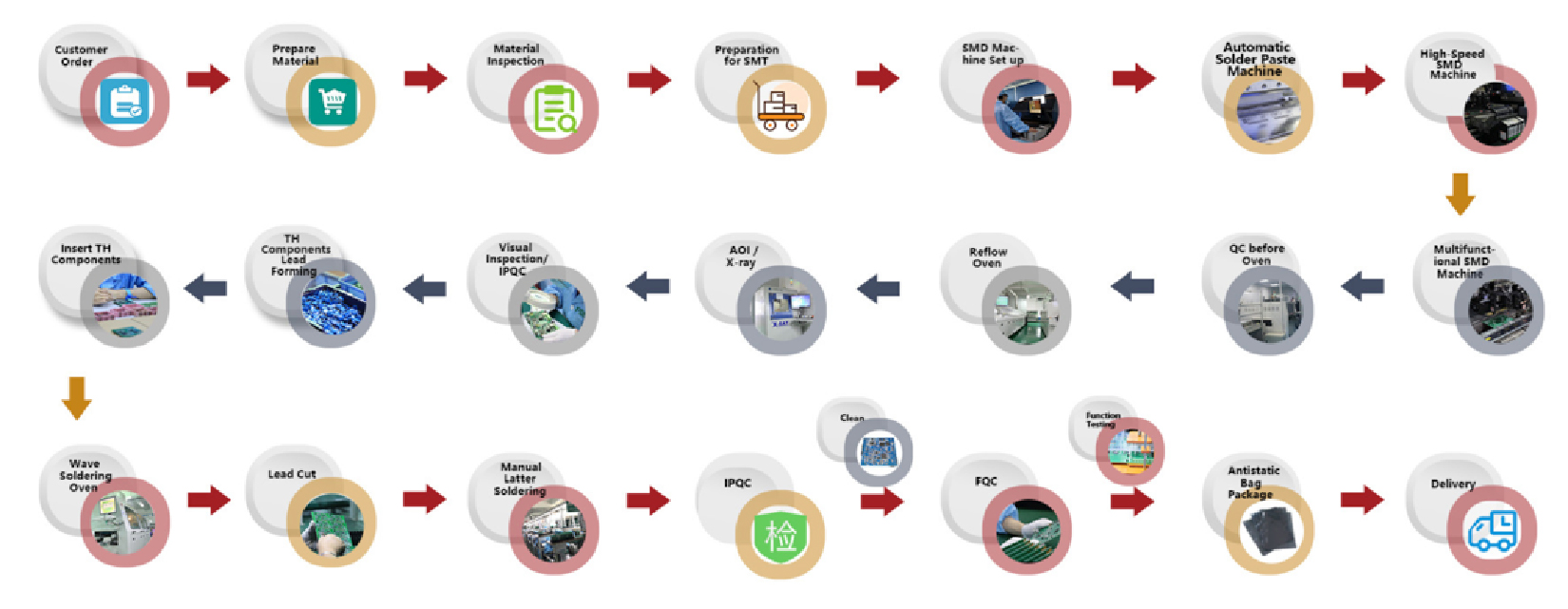
PCBA Process Flow

Complete PCBA assembly manufacturing process flow chart

PCBA Capacity

Our one-stop manufacturing solution covers all your PCB assembly requirements:
Order Volume: No minimum order quantity available. Support engineering prototypes and low-volume first article builds
Component Procurement: Turnkey Service, Consigned/Kitted Materials, Partial Turnkey
Assembly Types: SMT, Through-hole DIP, Mixed SMT & Through-hole Technology, Single/Double-sided Component Placement, Fine Pitch Components
 
Flexible Circuit Assembly
Solder Process: RoHS-compliant Lead-free soldering, No-clean process optional
Inspection Equipment: 2D SPI, Pre-reflow AOI, Post-reflow SMT AOI, X-Ray Inspection
Testing Services: Functional Testing, Humidity Test, High & Low Temperature Cycling, Salt Spray Test, Vibration Test, Shock Test
 
Key Technical Specifications:
Stencil dimension range: 1560 × 450mm
Minimum SMT Component: 01005
Minimum IC Lead Pitch: 0.3mm
Maximum PCB Size: 1200 × 400mm
Minimum PCB Thickness: 0.35mm
Maximum BGA Size: 74 × 74mm
BGA Ball Pitch: 0.4 ~ 1.0mm
BGA Ball Diameter: 0.45 ~ 0.76mm
QFP Lead Pitch: 0.38 ~ 2.54mm
PCBA assembly technical capacity parameter overview

PCBA Lead Time

We operate 6 automated high-precision SMT production lines equipped with Panasonic and Samsung equipment. The production lines support components down to 0201, QFP ranging from 0.6mm×0.3mm up to 50mm×50mm with 0.15mm lead gap and ±0.05mm placement accuracy. Daily component mounting capacity reaches 11,000,000 placements.
 
Our engineering team possesses rich experience in DFM/DFA/DFT analysis.
We provide in-house BGA rework, re-balling and X-Ray inspection services. Laser-cut stencils can be manufactured and delivered within 4 hours.
Order Type Standard Lead Time Fast-Track Lead Time
Prototype (<20pcs) 2 days 12 hours
Small Batch (20–100pcs) 6 days 24 hours
Medium Batch (100–1000pcs) 5 days 48 hours
Mass Production (>1000pcs) Subject to BOM availability Subject to BOM availability

PCBA Testing

We deploy advanced testing technologies and reliable PCB assembly manufacturing services to deliver premium products for global customers, covering the full workflow from design verification to shipment.
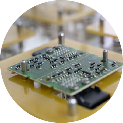
PCBA Functional Testing equipment

Functional Testing

Comprehensive testing in new product development cuts clients’ costs and reduces production downtime. Early-stage ICT, AOI and Agilent 5DX inspections provide key feedback for timely revisions. Custom functional and application testing is conducted per customer requirements, followed by environmental stress screening to verify long-term reliability. Bestech’s full functional testing solutions enable first-pass production success and deliver products beyond client expectations.
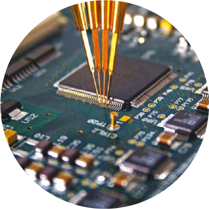
Flying Probe Test fixtureless ICT testing machine

Flying Probe Test (Fixtureless ICT)

AXI – 2D & 3D Automated X-Ray Inspection
AOI – Automated Optical Inspection
ICT – In-Circuit Test
ESS – Environmental Stress Screening
EVT – Environmental Verification Test
FT – Functional & System Test
Configure-to-order Assembly
Failure Analysis & Diagnostic Testing
Full PCBA Manufacturing & Test Solutions
ICT In-Circuit Comprehensive Testing equipment

ICT In-Circuit Comprehensive Testing

In-Circuit Testing (ICT) is widely adopted for mature products in electronic subcontract manufacturing. Bed-of-nails test fixtures access multiple test points on the bottom side of PCBs. With adequate test point coverage, ICT transmits high-speed test signals to evaluate individual components and circuit networks efficiently.

Testing Laboratory Equipment

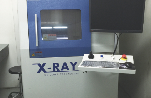
PCBA X-Ray Inspection System for BGA inspection
X-Ray Inspection System
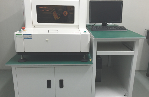
3D SPI Solder Paste Inspection machine
3D SPI Machine
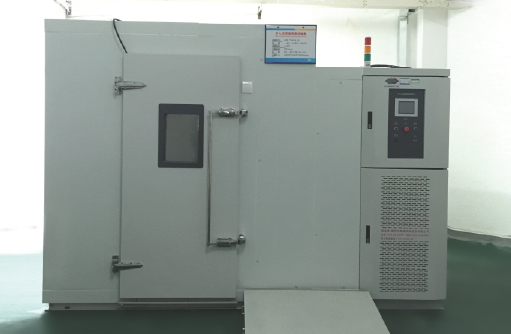
High low temperature test chamber for electronics reliability test
High & Low Temperature Test Chamber
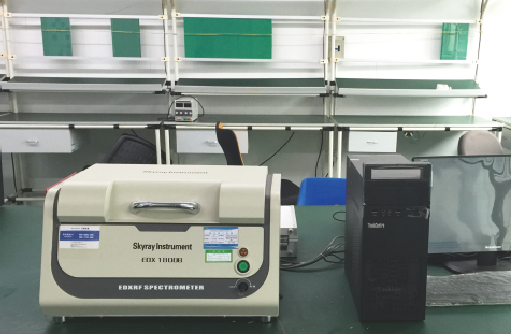
RoHS XRF Spectrometer material testing equipment
RoHS XRF Spectrometer
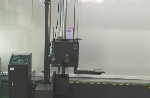
Drop test machine for electronic assembly reliability test
Drop Test Machine
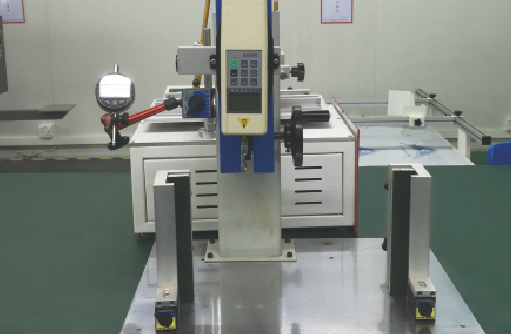
Push pull tester for component bonding strength testing
Push-Pull Tester

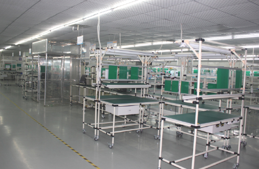
PCBA Production Facilities

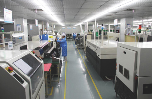
Automated SMD SMT production line workshop
14 × SMT Production Lines
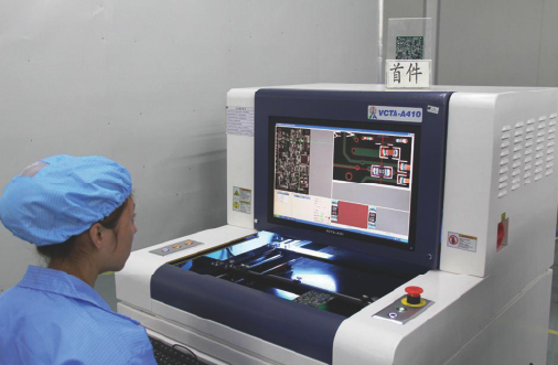
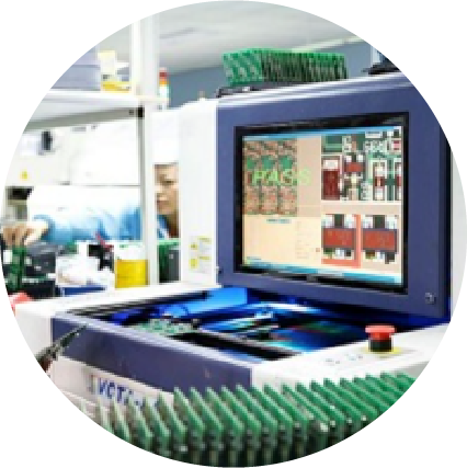
AOI automated optical inspection equipment for PCBA
13 × AOI Inspection Equipment
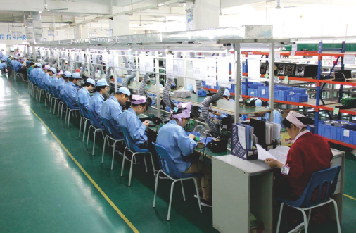
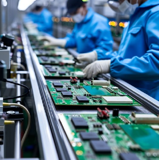
PCBA manual assembly production line
9 × Assembly Lines
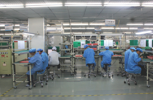
U-cell DIP through-hole assembly production line
20 × U-Cell DIP Lines
Selective conformal coating production line for circuit boards
Selective Conformal Coating Line
PCBA functional testing production line
24 × Functional Testing Lines