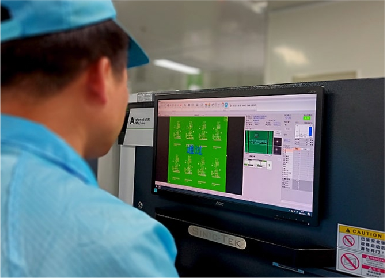
SPI acts as the first quality barrier in SMT manufacturing. It monitors solder paste printing before component placement. Early detection of printing defects improves first-pass yield and avoids expensive rework after reflow.
What it checks:
Solder paste volume, thickness and coverage area
Print offset, bridging or insufficient paste deposition
Stencil alignment accuracy
Key Advantages:
Prevent SMT defects in advance, reduce post-reflow rework
3D scanning technology accurately measures paste geometry
Provide data support to optimize stencil design and printing parameters
High-speed scanning without slowing down production tact time
Best for:
High-density PCBA with 0201 / 01005 components and fine-pitch BGA; high-reliability products requiring strict solder joint quality