



Home/Capabilities/Design and Engineering

What is PCB Design and Layout

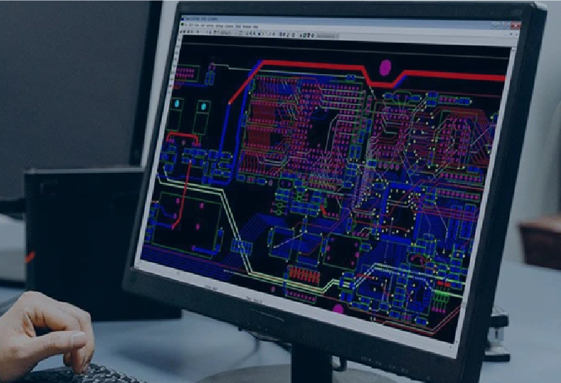
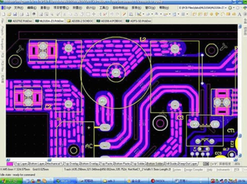
PCB design and layout refers to creating the physical layout of printed circuit boards for interconnecting electronic components. The workflow covers component placement, electrical signal routing, as well as board outline dimension definition. Bestech delivers comprehensive printed circuit board design services supported by an experienced engineering team, capable of handling PCB projects ranging from simple single-layer boards to highly complex high-speed multilayer designs. After layout completion, we support seamless handover to PCBA manufacturing and prototype validation.
 
Bestech PCB design and layout engineering service

Our PCB Design and Layout Services

Bestech owns mature professional design & engineering capabilities to deliver flexible customized design solutions. We provide full turnkey PCB design services. Clients only need to provide initial product concepts, and our team will develop feasible engineering solutions. Additionally, we support joint development together with customers’ internal engineering teams. Our engineers conduct thorough design feasibility reviews to mitigate risks and improve end-product reliability. We also support fast prototyping to accelerate your product time-to-market, paired with premium manufacturing enabled by advanced production technology.

PCB Design Service Scope at Bestech

Schematic Design
We develop complete electronic schematics according to functional requirements, including circuit architecture design, component selection and net definition for industrial, automotive and consumer electronic products.
PCB Layout Design
Precise component placement, high-speed signal routing, ground/power plane design, layout optimization for electrical performance and manufacturability.
Library Creation
Custom schematic symbols, PCB footprints and 3D component model development, ensuring consistency and accuracy throughout design iterations.
Prototype Assembly & Testing
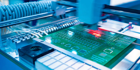
PCB prototype fabrication, SMT assembly and functional testing to validate circuit functionality, performance and stability before mass production.
Design Review & Optimization
Comprehensive DFM, SI, PI and EMI review to identify layout risks and optimize design for cost, yield and long-term reliability.

PCB Design Capabilities

Comprehensive Design Capabilities:
  • Mixed technology, SMT & through-hole hybrid PCB designs
  • Micro BGA, Micro Via, Blind & Buried Via implementation
  • Analog and Mixed-Signal PCB Design
  • High-speed Digital PCB Design
  • RF & Microwave Layout Design
  • Low-noise sensitive analog circuit layout
  • PCB Reverse Engineering Service
  • Signal Integrity Simulation & Design Verification
  • EMI/EMC Analysis & Optimization
  • Design compliance engineering support
Supported PCB CAD Software Platforms
  • Altium Designer
  • Mentor Graphics (Xpedition)
  • CADSoft EAGLE
  • PADS
  • Cadence Allegro

Technical Capabilities

Category Capabilities
Product Types Automotive electronics, instrument clusters, cockpit domain controllers, industrial control systems, networking & communication equipment, instrumentation, test systems, display devices, etc.
Chip Types Mainstream ARM processors (domestic & international), MCUs, DSPs, radio tuners, audio amplifiers, power ICs, DDR3~DDR5, 4G/5G communication chips, etc.
PCB Types Standard rigid PCBs, HDI boards, flexible PCBs
Design Standards Compliant with IPC-2221 and IPC-7351; implementing DFM, DFA, and DFT principles
Maximum Design Layers Up to 20 layers
Minimum Via Size 4 mil
Minimum Trace Width 2.5 mil
Minimum Trace Spacing 2.5 mil
Maximum Board Density 0.01
Maximum Component Count 10,000+
Maximum Pin Count 30,000+
Wide Temperature Design -40°C ~ 105°C
High-Speed Design Up to 22 Gbps
FCT Coverage 100%
ICT Coverage 100%

PCB Design and Layout FAQs

PCB design engineer technical consultation FAQ