Home/Service/PCB

PCB Fabrication

Bestech provides turnkey PCB manufacturing services headquartered in Shenzhen, delivering high-quality rigid circuit boards at competitive prices. We support both PCB prototype and mass production ranging from 2 layers up to 32 layers. Backed by our parent company Bestech Electronics in China, customers obtain obvious advantages: shorter lead times, lower manufacturing costs, and strict localized quality control management. All PCB manufacturing files undergo complete CAM review before production, and every finished printed circuit board complies with IPC-A-600 Class 2 or higher standards. Request your instant online PCB quote or contact our sales engineers directly for further inquiries.

Production Range:

  • Layer Count: 2–32 layers (rigid PCBs)
  • Materials: FR-4 (High Tg, Low CTE), high-frequency laminates, metal core substrates, embedded passive materials
  • Surface Finishes: HASL, LF HASL, ENIG, Immersion Tin, Immersion Silver, Gold Fingers

Advanced PCB Capabilities:

  • HDI PCBs
  • Metal Core PCBs
  • High-frequency materials & FR4 Multilayer Laminates
  • Buried & Blind Holes, Controlled Impedance Boards

PCB Application Range:

  • Communications & Industrial Control Equipment
  • Computers & Peripherals
  • Automotive Electronics
  • Medical Equipment
  • Power Supplies
  • Aerospace Devices
  • Consumer Electronics

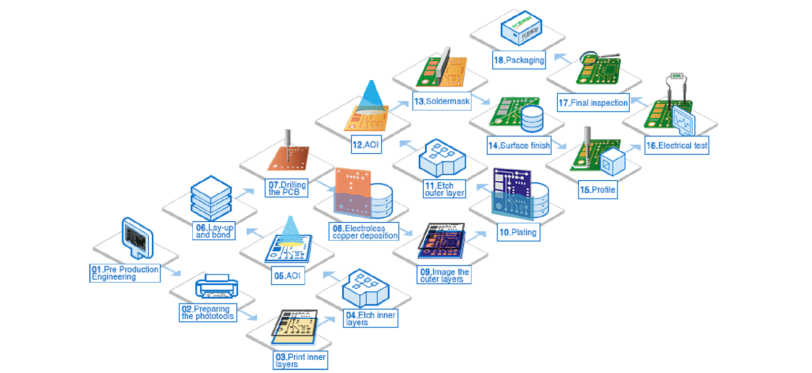
PCB Process Flow

PCB fabrication complete production process flow chart

PCB Production Capacity

Items Samples (PCB Prototypes) Capabilities (Mass Production)
Layer count 1–30L 1–16L
Board Thickness 0.2–7.0mm 0.4–6.0mm
Maximum Board Size 610×100mm 550×650mm
Copper Weight Inner Layer: 0.5–2 oz; Outer Layer: 0.5–3 oz Inner Layer: 0.5–2 oz; Outer Layer: 0.5–2 oz
Minimum Finished Hole Size 0.1mm 0.15mm
Hole Diameter Tolerance PTH: ±0.05mm; NPTH: ±0.05mm PTH: +0.075mm; NPTH: ±0.05mm
Maximum Aspect Ratio 16:1 10:1
Minimum Line Width 3.0 mil 4.0 mil
Minimum Line Spacing 3.0 mil 4.0 mil
Outline Dimension Tolerance ±0.10mm ±0.15mm
Maximum Allowable Bow & Twist 0.50% 0.75%
Solder Mask Color Green, Yellow, Black, Blue, Red, White, Purple Green, Yellow, Black, Blue, Red, White, Purple
Minimum Solder Mask Dam 4mil(Green), 5mil(Other colors) 4mil(Green), 5mil(Other colors)
Silkscreen Color White, Yellow, Black White, Yellow, Black
HASL Tin Thickness 2–40μm 2–40μm
Flash Gold (Electroplated Gold) Ni: ≥3μm; Au:0.025–0.1μm Ni: ≥3μm; Au:0.025–0.1μm
ENIG Ni: 3–8μm; Au:0.05–0.1μm Ni: 3–8μm; Au:0.05–0.1μm
Immersion Tin ≥1.0μm ≥1.0μm
Immersion Silver 0.2–0.4μm 0.2–0.4μm
OSP 0.1–0.3μm 0.1–0.3μm
Hard Gold 0.1–0.4μm 0.1–0.4μm
ENEPIG Ni:3–8μm; Pd:0.05–0.15μm; Au:0.05–0.1μm Ni:3–8μm; Pd:0.05–0.15μm; Au:0.05–0.1μm
Carbon Ink 0.10–0.35μm 0.10–0.35μm
Peelable Solder Mask 0.2–0.50μm 0.2–0.50μm
Raw Material FR-4, High Tg FR-4, Halogen-Free, PTFE, Aluminum Base Material, Ceramic-Filled Laminates FR-4, High Tg FR-4, Halogen-Free, PTFE, Aluminum Base Material, Ceramic-Filled Laminates
Surface Treatments Available Sn-Pb HASL, Lead-Free HASL, Flash Gold, ENIG, Immersion Tin, Immersion Silver, OSP(Entek), Hard Gold, Soft Gold, ENIG+OSP, ENIG+Gold Fingers, Hard Gold+Gold Fingers, Immersion Silver+Gold Fingers, Immersion Tin+Gold Fingers, ENEPIG Sn-Pb HASL, Lead-Free HASL, Flash Gold, ENIG, Immersion Tin, Immersion Silver, OSP(Entek), Hard Gold, Soft Gold, ENIG+OSP, ENIG+Gold Fingers, Hard Gold+Gold Fingers, Immersion Silver+Gold Fingers, Immersion Tin+Gold Fingers, ENEPIG

PCB Lead Time

Our target PCB on-time delivery rate reaches 98.5%
Service Principle
Quotation provided within 2 hours. Our engineers and technicians deliver responsive technical support throughout your whole PCB project cycle.
 
On-Time Delivery Commitment
We offer practical, optimized and cost-effective PCB manufacturing solutions for your printed circuit boards.
Layers Urgent Lead Time (PCB Prototypes) Standard Lead Time (PCB Prototypes) Lead Time (PCB Mass Production)
1–2 1 day 6 days 2 weeks
4 2 days 7 days 2 weeks
6 3 days 8 days 2.5 weeks
8 4 days 10 days 3 weeks
10 5 days 12 days 3 weeks
12 6 days 12 days 3 weeks
14 8 days 13 days 4 weeks
16–20 10 days 15 days 4 weeks

PCB Production Facilities

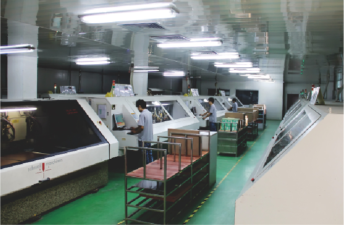
PCB Drilling Production Line equipment
Drilling Production Line
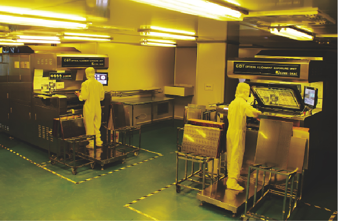
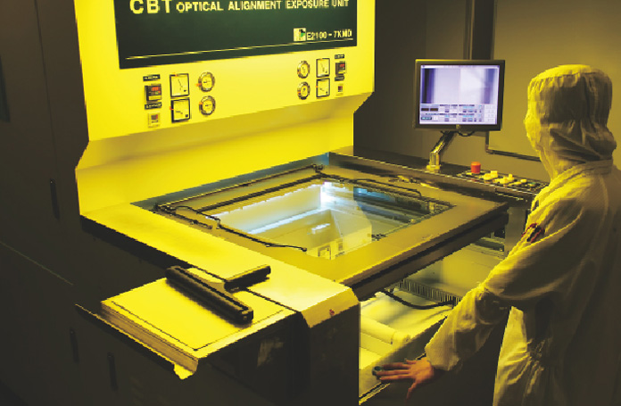
PCB Automatic Exposure Machine workshop
Automatic Exposure Machine
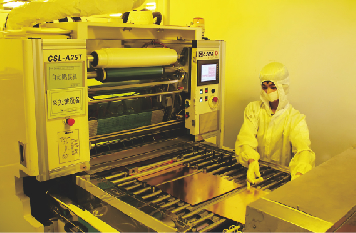
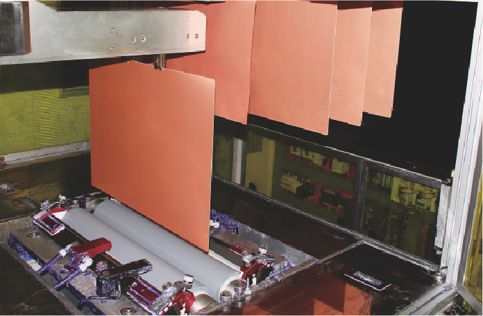
PCB Automatic Dry Film Laminator production equipment
Automatic Dry Film Laminator
PCB Pattern Transfer Equipment in production workshop
Pattern Transfer Equipment
PCB Automatic Solder Mask Coating production line
Automatic Solder Mask Coating Line
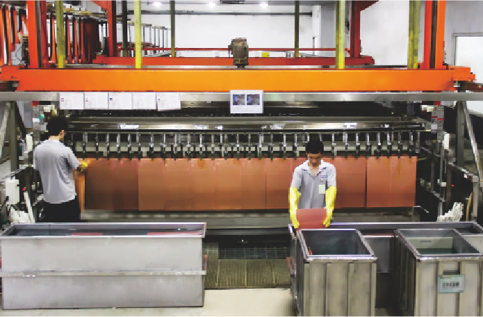
PCB Copper Plating Production Line equipment
Copper Plating Production Line